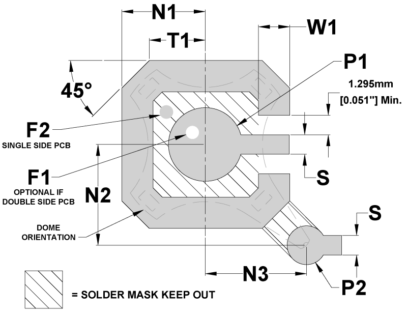
**NOTE**
-
Via hole through the board is suggested for venting if other means are not used
-
Snaptron recommends that the circuit area under the dome be void of solder mask. The keep out area begins at the outside edge of the outer circuit pad that the dome is positioned on and includes area inside of the pads.
This drawing represents one of many possible layouts. Snaptron conveys this information for customer support with the intent that the customer will be responsible for the final design of the PCB layout.
Dimensions
| Diameter | P1 | P2 | W1 | T1 | S | N1 | N2 | N3 | F1 | F2 |
|---|---|---|---|---|---|---|---|---|---|---|
| 8.5mm | 3.48mm (0.1370″) | 1.85mm (0.073″) | 1.55mm (0.061″) | 2.77mm (0.109″) | 0.92mm (0.036″) | 4.19mm (0.165″) | 4.87mm (0.192″) | 4.87mm (0.192″) | 0.89mm (0.035″) | 0.89mm (0.035″) |
| 10mm | 4.09mm (0.161″) | 2.16mm (0.085″) | 1.74mm (0.069″) | 3.10mm (0.122″) | 1.08mm (0.043′) | 4.63mm (0.182″) | 5.59mm (0.220″) | 5.62mm (0.221″) | 0.89mm (0.035″) | 0.89mm (0.035″) |
| 12mm | 4.90mm (0.193″) | 2.54mm (0.100″) | 2.08mm (0.082″) | 3.72mm (0.146″) | 1.30mm (0.051″) | 5.55mm (0.218″) | 6.71mm (0.264″) | 6.74mm (0.265″) | 0.89mm (0.035″) | 0.89mm (0.035″) |
| 14mm | 5.70mm (0.224″) | 3.07mm (0.121″) | 1.98mm (0.078″) | 4.34mm (0.171″) | 1.60mm (0.063″) | 6.40mm (0.252″) | 7.97mm (0.314″) | 7.97mm (0.314″) | 0.89mm (0.035″) | 0.89mm (0.035″) |